CSCI 2150 -- Laboratory Experiment 8
LabView: Chip Select Design
Due: MW sections -- March 29; TH sections March 30
The purpose of this homework is to give you an opportunity to design chip selects. A review is presented below on chip selects to assist you in completing this assignment.
By the end of this homework assignment, you will have designed the logic for the three chip selects so that the memory range for each chip select is equal to that shown below.| Chip Select | Low Address | High Address |
CS1 |
000016 |
3FFF16 |
CS2 |
800016 |
87FF16 |
CS3 |
C00016 |
CFFF16 |
Chip Select Review
The need for memory mapping (assigning different components of memory to different portions of the memory map) arises from the need to have multiple memory devices accessible across a single address/data bus. Therefore, we need to have a method of setting the "base" or "starting" address of a memory device to an address other than 0. For example, the memory map below has a ROM starting at address 0x1000, a RAM starting at 0x4000, and a piece of memory-mapped I/O starting at address 0xC000.
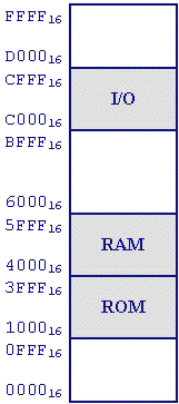
Note that different devices can take up different amounts of memory. As long as there is no overlap in the ranges and as long as the low address and the high address of a range are valid, the devices can co-exist on a single bus.
Let's start by reviewing the basic structure of a memory chip. The figure below shows the basic components of a memory chip.
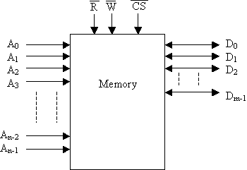
It has n input address lines, therefore, the size of the memory is 2n. It has m data lines, and therefore can store m bits of data for each address. The main lines of control for the memory are ^R, ^W, and ^CS. When ^R is low, the processor is reading from the memory and the memory should be outputting data on its data lines. When ^W is low, then the processor is writing data and the memory should be inputting data to store in the memory cells.
If ^CS is high, the data lines of the chip are disabled. It is as if the chip is not even connected. When ^CS is low, the data lines are enabled for input or output based on the state of ^R and ^W. It is this ^CS line that enables multiple devices to be connected to a single set of data lines as shown in the image below.

As far as the processor is concerned, it has n output address lines where this n must be at least as large and most likely larger than the n input address lines to the memory chip. In this case, n gives you the size of your memory space (the number of memory locations addressable by the processor) and is once again calculated as 2n. It also has m labeled D0 through Dm-1 where m is the number of bits of data. This m should be the same value as the m on the memory chips.
Creating a Chip Select
Assume we have a 1 Meg address space. (I.e., the processor can address up to 1,048,576 memory spaces.) How many address lines does the processor have?
220 = 1,048,576

Therefore, the processor has 20 output address lines
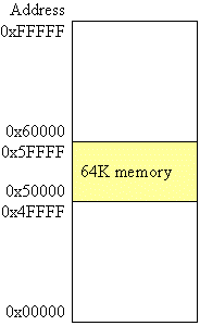
Assume we want to insert a 64K (65,536 memory addresses) RAM starting at address 0x50000. First, how many address lines does the 64K memory chip have?
216 = 65,536

Therefore, the memory has 16 input address lines
First, convert the hexadecimal low address of 0x48000 to binary.
| Hexadecimal | 4 | 8 | 0 | 0 | 0 |
| Binary | 0100 | 1000 | 0000 | 0000 | 0000 |
Now, divide the processor's address lines into the addresses that will be input to the memory and the addresses that will be used to create the chip select.
| A19 | A18 | A17 | A16 | A15 | A14 | A13 | A12 | A11 | A10 | A9 | A8 | A7 | A6 | A5 | A4 | A3 | A2 | A1 | A0 |
| 0 | 1 | 0 | 1 | 0 | 0 | 0 | 0 | 0 | 0 | 0 | 0 | 0 | 0 | 0 | 0 | 0 | 0 | 0 | 0 |
| The chip select will use these 4 lines |
These 16 address lines must go to memory chip |
||||||||||||||||||
Note that ALL of the lines going to the memory chip MUST BE ZERO in order for this to be used as the low address of the memory range. If this is not true, you will need to adjust the low address so that the memory chip receives all zeros when the low address is used by the processor.
Next, we need to figure out what the high address will be for the 64K memory. It will be the address where all of the address lines going to the memory, A0 through A15, are one. That value is binary 0101 1111 1111 1111 1111 which equals 0x5FFFF in hexadecimal. The resulting memory map is shown below.
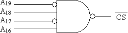
The remaining address lines (the ones that come from the processor but do not go to the memory chip) are used to enable or disable the memory chip by creating the chip select circuit. To do this, we need to make a chip select that is a logic zero only when A19 = 0, A18 = 1, A17 = 0, and A16 = 1. Using a NAND gate as we have in class for the 1-of-x selectors, we get:
Designing the Chip Selects
Now let's get back to the homework. I want you do to four things:
- determine the memory space of the microprocessor with 16 address lines;
- determine the size of each of the blocks of memory defined with the
chip selects shown below;
Chip Select Low Address High Address CS10000163FFF16CS280001687FF16CS3C00016CFFF16
- verify that both the low and high addresses are valid for each of the memory blocks; and
- design the chip selects.
Developed by David Tarnoff sections of CSCI 2150 at ETSU