Although the set of notes you have requested is presented below, it has not been maintained since January, 2003. All of the information in these notes has been included in an on-line text titled Computer Organization and Design Fundamentals. The book is available in three formats, two of which are free electronic downloads. Please visit one of the following links in order to access the format you prefer.
Thank you for your interest in this textbook. Please feel free to e-mail me at tarnoff etsu.edu if you have any questions or comments.
-Dave Tarnoff
Reading: Digital Fundamentals section 14.3
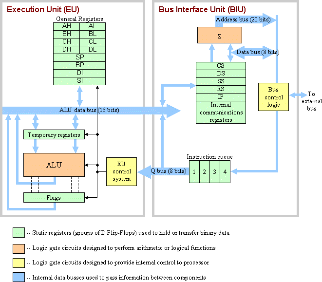
Below is a block diagram of the organizational layout of the Intel 8088 processor. It includes two main sections: the Execution Unit (EU) and the Bus Interface Unit (BIU). The EU takes care of the processing including arithmetic and logic. The BIU controls the passing of information between the processor and the devices outside of the processor such as memory, I/O ports, storage devices, etc.
The rest of this document will describe the purpose of the different portions of the processor within these two units.
The general registers are categorized into two sets: data and address. The data registers are for calculations; the address registers contain memory addresses and are used to point to the locations in memory where data will be retrieved or stored.
Examining the diagram shows that there are four pairs of registers at the top labeled AH, AL, BH, BL, CH, CL, DH, and DL. These are the data registers. Each of these registers is 8 bits long. Each pair, however, can also operate as a single 16 bit register. AH and AL can operate as a pair referred to as AX. This combining of registers is simply a concatenation, the 8 bits of AL simply tacked to the end of the 8 bits of AH. For example, if AH contains 101100002 (B016) and AL contains 010111112 (5F16), then the virtual register AX contains 10110000010111112 (B05F16).
Example: If CX contains the binary value 0110 1101 0110 10112, what value does CH have?
Answer: CH contains 0110 11012.
Intel has given each of these computational registers a name. These names are listed below:
Below the data registers in the block diagram are the address registers: SP, BP, DI, and SI. These are officially referred to as the pointer (SP and BP) and index registers (DI and SI). These registers are used with the segment registers to point to specific addresses in the memory space of the processor. We will address their operation in the section on the segment registers. It is sufficient at this point to say that they act like pointers in the programming language C or C++. Their basic function is as follows:
Imagine the instrumentation on the dash board of a car. Blinking on and off occasionally behind the speedometer, tachometer, fuel gauge, and such, are a number of lights informally called "idiot lights". Each of these lights has a unique purpose. One comes on when the fuel is low. Another lights up when the high beams are on. Another warns the driver of low coolant. There are many more lights, and depending on the type of car you drive, some may even replace a gauge such as oil pressure.
Now let's go back to the processor. There are a number of "idiot lights" that the processor can use, each one based on the result of the previous operation. For example, the addition of two number might produce a negative sign, an erroneous overflow, a carry, or a value of zero. Well, that would be four idiot lights: sign, overflow, carry, and zero.
Each of these idiot lights, otherwise known as flags, can be represented with a single bit. If the resulting number had a negative sign, the sign flag would equal 1. If the result was not a negative number, (zero or greater than zero) the sign flag would equal 0. (Side note: Motorola processors more correctly refer to this flag as the negative flag.)
For the sake of organization, these flags are grouped together to form a single number. That number is the flags register shown at the bottom of the EU section of the processor diagram. The individual bits of the flags are arranged as shown in the figure below:
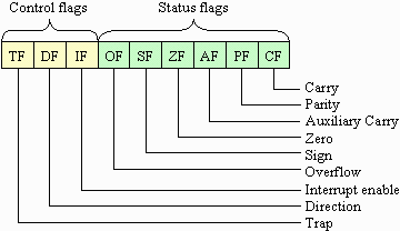
The group of flags in the figure identified as control flags are used to control how the processor runs. These are typically controlled by the user's software. The group of flags in the figure identified as status flags are usually set by the previous operation as in our addition example.
Example: Assume the flag register is set as shown below after an addition. Using these flags, what can you tell us about the result?
| TF | DF | IF | OF | SF | ZF | AF | PF | CF |
| 0 | 0 | 0 | 0 | 1 | 0 | 0 | 0 | 1 |
Answer: As a result of the addition, there was no overflow (OF=0), the result is negative (SF=1), it isn't zero (ZF=0, but you could've also told us that because it is negative), and there was a carry.
Example: If you were to add the binary number 101101012 and 100101102, how would the flags be set?
Answer: First, let's add the two numbers to see what the result is.
  1 0 1 1 0 1 0 1

+ 1 0 0 1 0 1 1 0
1 0 1 0 0 1 0 1 1
Now just go from left to right through the status flags.
As implied by the name, the Arithmetic Logic Unit (ALU) is the computation portion of the EU. Any time arithmetic or logic needs to be performed on numbers, the numbers are sent from the general registers to the ALU, the ALU performs the function, and the result is sent back to the general registers.
The EU Control System is a set of gates that control the timing, passing of data, and other items within the execution unit. It's analogous to a manager in business who doesn't necessarily know the details of the operation, but they plan what happens, where it happens, and when it happens.
The Instruction Pointer (IP) can be found toward the bottom of the group of registers in the center of the BIU. This register is an address register just like the SP, BP, DI, and SI registers in the EU. The difference is its purpose. The IP points to the next instruction to execute from memory. I will elaborate on this in the section on segment registers.
In the center of the BIU section of the processor organizational block diagram is a set of registers labeled CS, DS, SS, and ES. These four registers are the segment registers and are used in conjunction with the pointer and index registers to store and retrieve items from the memory space.
My anal readers probably noticed that our address registers are 16 bits wide while the address space of the 8088 is 20 bits. (The memory space of the original 8088 is 220 = 1 Meg.) So how does this work? Are four of the address lines just ignored since we can only send 16 bits of information from our addressing registers? Of course not.
Next time your Windows operating system throws up an error, look to see if it gives you the address where the error occurred. If it does, you should see a number that looks something like:
3241:A34EThis number is actually the combination of 2 registers: a segment register (the number to the left of the colon) and a pointer or index register (the number to the right of the colon). Note that a four digit hexadecimal number results in a 16 bit binary number. It is the combination of these two 16-bit registers that creates the 20-bit address line.
To do this, take the value in the segment register and shift if left four places, i.e., add four zeros to the right side of the number. In our example above, 324116 = 0011 0010 0100 00012 becomes 3241016 = 0011 0010 0100 0001 00002. This value is then added to the pointer or index register. This makes the value from our example:
  0011 0010 0100 0001 0000 (hexadecimal 32410)

+      1010 0011 0100 1110 (hexadecimal A34E)

  0011 1100 0111 0101 1110 (hexadecimal 3C75E)
This computation takes place in the "Address Summing Block" located directly above the segment registers in the BIU in the organizational block diagram.
Therefore, the process of trying to access a single location in the 8088 processor's memory space takes three things:
If we look at this from the memory space point of view, the segment register shifted left four places so that four zeros are filled in from the right points to an address somewhere in the memory space. The offset address is then added to it to point to an address within the 216 = 65,535 (64K) locations above where the segment register is pointing.
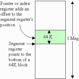
There are two purposes for this summation of segment and pointer registers to access a single, physical memory address. First, it allows the processor to access more address lines (20 in the case of the 8088) than it has bits in its address registers (16 in the case of the 8088).
There is, however, a more significant reason, a reason that allows you to load multiple programs at one time. It is called relocatable code. Let's put it this way, if you're loading both Microsoft Word and Netscape at the same time, does it matter which one you load first? Of course not.
The way this works is that the program itself has control of the pointers and index registers. It's as if they have a 64K block of memory to jump around in wherever they want. The operating system, however, has control of the segment registers. That way it can force a program to reside in a specific segment of memory. As long as the segment value stays the same for that program, and the program only manipulates the pointer and index registers, then there will be no errors. When something messes up one of these registers so that the physical address being pointed to is outside the allowed range for the program, that's when the "blue screen of death" appears.
Each segment register has its own name as shown below:
Some of the segment registers and pointer registers are set up to operate in pairs for a specific purpose. These are:
The Bus Control Logic is a set of gates that control access to the external bus of the 8088. This includes all external memory devices, I/O ports, and other resources that communicate with the processor through the bus.
Microprocessor designers, in an attempt to squeeze every last bit of speed from their designs, try to make sure that every circuit is doing something productive at all times. If their is an idle circuit, then try to see if it can't predict what it should be doing and perform that function. If it predicted wrongly, then through the result away. If it predicted correctly, then time was saved and code was executed faster.
The most popular application of this theory is with the execution of the machine code instructions. In general, the execution of a machine code instruction can be broken into three stages:
When examining the architecture of the 8088 processor, you may notice that there are three separate circuits which perform these three tasks.
If the bus control logic is done fetching the current instruction, what's to keep it from fetching the next instruction? It may have to guess what the next instruction is, but if it guesses right, then the EU control system won't have to wait for the next instruction to be fetched once it's completed the execution of the current instruction.
And once the EU control system has finished telling the ALU what to do to execute the current instruction, what's to keep it from decoding the next instruction while it's waiting for the ALU to finish? If the bus control logic guessed right about what the next instruction is, then the ALU won't have to wait for a fetch and subsequent decode in order to execute the next instruction.
This is called pipelining, and it is an important method for speeding up the operation of a processor.
Keeping with our simple three part process for executing an instruction, the example below shows how much time can be saved with pipelining. (Note: "F" represents the fetch cycle, "D" represents the decode cycle, and "E" represents the execute cycle. The subscript after the letter indicates the instruction number.)
Processor operation without pipelining
| cycle | 1 | 2 | 3 | 4 | 5 | 6 | 7 | 8 | 9 | 10 | 11 | 12 | 13 | 14 | 15 |
| process | F1 | D1 | E1 | F2 | D2 | E2 | F3 | D3 | E3 | F4 | D4 | E4 | F5 | D5 | E5 |
Without pipelining, five instructions take 15 cycles to execute. Now let's see how fast those same five instructions are executed using a pipelined architecture.
Processor operation with pipelining
| cycle | 1 | 2 | 3 | 4 | 5 | 6 | 7 |
| process | F1 | D1 | E1 | F2 | D2 | E2 | F3 | D3 | E3 | F4 | D4 | E4 | F5 | D5 | E5 |
Fifteen cycles reduced to seven. That's quite an improvement. If this pipelining thing works, it can make the processor appear a great deal faster. In fact, the following equations represent the difference.
number of cycles(non-pipelined) = 3 * number of instructions

number of cycles(pipelined) = 2 + number of instructions
Therefore, if the number of instructions is quite high, the number of cycles required of a pipelined architechture is almost 1/3 of that of the non-pipelined.
Example: What is the difference in the number of cycles required to execute 50 instructions between a pipelined and a non-pipelined processor?
Answer:
number of cycles(non-pipelined) = 3 * 50 = 150 cycles

number of cycles(pipelined) = 2 + 50 = 52 cycles
The Instruction Queue is the mechanism in the Intel 8088 processor that handles the pipelining function.
Notes developed by David Tarnoff solely for use by students in his sections of CSCI 2150.