Although the set of notes you have requested is presented below, it has not been maintained since January, 2003. All of the information in these notes has been included in an on-line text titled Computer Organization and Design Fundamentals. The book is available in three formats, two of which are free electronic downloads. Please visit one of the following links in order to access the format you prefer.
Thank you for your interest in this textbook. Please feel free to e-mail me at tarnoff etsu.edu if you have any questions or comments.
-Dave Tarnoff
Topic: After today's discussion, you should have a general idea of how memory is organized internally, the characteristics of different types of memory, and how memory is interfaced into the computer.
Reading: Digital Fundamentals, Sections 12.1-12.6
Data in memory are stored in arrays of "cells". Each cell contains a single bit, and as you know, each bit can contain either a 1 or a 0.
(The following was distilled from Intel Museum -- Memory Technology)
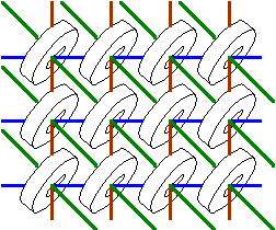
The first type of computer memory was called magnetic core memory. It was made by weaving copper wires through rings of magnetic material in an array. (See the figure below.) The combination of rows (blue lines), columns (brown lines), and diagonals wires (green lines) were used to set a magnetic field to the individual rings. There were two possible directions for the magnetic field in the rings: clockwise (a logic 1) and counter clockwise (a logic 0). A single bit of the data could then be retrieved by reading the column and row (address) of the bit you were interested in.
Modern memory has the same basic configuration although the magnetic core cells have been replaced transistors, and in the case of many types of RAM, each core cell is simply a D Flip-Flop.
|
A2
|
A1
|
A0
|
X0
|
X1
|
X2
|
X3
|
X4
|
X5
|
X6
|
X7
|
|
0
0
0
0
1
1
1
1
|
0
0
1
1
0
0
1
1
|
0
1
0
1
0
1
0
1
|
0
1
1
1
1
1
1
1
|
1
0
1
1
1
1
1
1
|
1
1
0
1
1
1
1
1
|
1
1
1
0
1
1
1
1
|
1
1
1
1
0
1
1
1
|
1
1
1
1
1
0
1
1
|
1
1
1
1
1
1
0
1
|
1
1
1
1
1
1
1
0
|
There are many different functions of memory in the operation of a computer. If we expand our discussion to all processor applications, then the functions of memory become even more numerous. In order to understand what memory technology to apply to which processor operation, we need to understand a little bit more about the technologies themselves.
The first step in understanding the different memory technologies is to understand some memory terminology.
In every computer system, there must be a portion of memory that is stable, not corruptable, and impervious to power loss. Without this memory, you would never be able to unplug the computer, and in the case of a rampant corruption of memory, you may never be able to boot the computer again. This kind of memory is called Read Only Memory or ROM.
In general, a processor cannot write to this type of memory. Of course there must be some mechanism in place that allows data to be written to this memory in the first place, but typically, the processor will generate an error if a program attempts to store data to this type of memory.
Since a processor cannot alter the data in a ROM, ROMs are used to store data that the microprocessor only reads. Examples include:
There are some types of ROMs that the microprocessor can write to, but usually the time needed to write to them or the programming requirements needed to do so make it unwise to write to them regularly. Therefore, the memories are still considered read only.
Random Access Memory (RAM) is easily read from and written to by the microprocessor. This allows them to act as:
Typically, they are very fast both for reading and writing. They also tend to be volatile in that as soon as power is removed, all of the data is lost.
For as long as memory has existed, scientists and engineers have tried to modify the technologies in order to make RAM faster and to cram more of it into a smaller space. This has resulted in two primary types of RAM, Static RAM (SRAM) and Dynamic RAM (DRAM).
SRAM is created by taking an array of latches such as the D-latch we studied earlier. Each D-latch can maintain a single bit of data within a single memory address or location. For example, if a memory stores eight bits per memory address, then there are eight latches for a single address. If this same memory has an address space of 16K = 214, then there are 214*8 = 217 = 128K latches in the device.
Latches are not small devices as logic circuits go, but they are very fast. Therefore, in the pursuit of the performance goals of speed and size, SRAMs are better adapted to speed.
A bit is stored in a DRAM using a device called a capacitor. A capacitor is made of a pair of metal plates that are held parallel and very close together, but not touching. If an electron is placed on one of the plates, its negative charge will force an electron on the other plate to go away much as the north pole of a magnet will push away the north pole of a second magnet.
If enough electrons are deposited on the one plate creating a strong negative charge, enough electrons will be moved away from the opposite plate creating a positive charge. And like a north pole attracting the south pole of a second magnet, the charges on these two plates will be attracted to each other and maintain their charge. This is considered a logic '1'. No charge is a logic '0'.
Since a capacitor can be made very small, DRAM technology is better adapted to high density memories, i.e., cramming a great deal of bits into a small space.
There is a problem though. Every once in a while, one of the electrons will escape from the negatively charged plate and land on the positively charged plate. This exchange of a negative charge decreases the overall charge difference on the two plates. If this happens enough, the stored '1' will disappear. This leakage of electrons from one plate to the other is referred to as leakage current.
Electrons are lost too when the processor reads the data. It takes some level of energy to pull data out of the DRAM and that energy is the stored electrons.
In order to avoid having leakage current or processor reads corrupt the data stored on the DRAMs, (i.e., turning the whole mess to zeros) additional logic called refresh circuitry is used that occasionally reads the data in the DRAM then restores it with a full charge of electrons to the capacitors storing ones. This logic also recharges the capacitors when the processor reads data. The refresh circuitry makes the process of keeping data valid on the DRAMS transparent to the processor.
In general, SRAMs:
There are circuits that allow SRAMs to be connected to a back up battery that allows the data to be stable even with a loss of power. These batteries, slightly larger than a watch battery, can maintain the data for long periods of time much as a battery in a watch can run for years. On the negative side, the extra battery and circuitry adds to the overall cost and takes up board space.
In general, DRAMs:
In the logic circuits that we have been designing, once you place the inputs on a circuit, the outputs appear after a short delay. Well, memories have inputs including address lines, input data lines, and control lines and outputs on which to put data. Asynchronous memory works much like our logic circuits in that the inputs are processed, and after a short delay, an output results.
This makes it very tough on the circuit board designers that design motherboards. The have to run the processor slower to allow for the ambiguous timing of the memories. The memory may be ready with the data before the processor needs it, but data from a different address may take a while longer to be retrieved.
Some processors, however, are designed so that the memory follows a precise timing requirement. This timing is governed by a clock that is added to the bus keeping everything that is attached to the bus in lock-step. Memories that are connected to this type of bus are referred to as synchronous memory. The ability of the processor to predict exactly when data will be ready on the bus allows it to adhere to more precise timing requirements, and therefore run faster.
If two RAMs are made with the same technology, the larger memory will take longer to find a piece of data. This is mostly due to delays within the address decoder. In addition, recall that a memory will be faster if it is made with SRAM rather than DRAM.
To make a computer run faster, many architectures add a small SRAM called a cache memory or a cache RAM between the big main memory and the processor. When a piece of data is used from the larger memory, it is copied into the smaller memory so that next time it is needed, it will be quicker to access. As the cache fills, older pieces of data are discarded in favor of storing newer data.
The process of storing the data, organizing it in the cache, and determining which data to discard are all design options the need to be taken into consideration when designing caches.
As far as reading data goes, the processor treats every memory device exactly the same. On the bus, the processor first places the address it wishes to retrieve data from on the address lines, pulls the read control line (^R) low, then reads the data from the data lines.
The process of writing data to a RAM is similar. On the bus, the processor first places the address it wishes to store the data to on the address lines, it places the data to be stored on the data lines, then it pulls the write control line (^W) low which latches the data into the RAM.
By nature, since ROMs are intended primarily for reading data, the procedure used to store data to the devices is not usually the duty of the processor. There are a number of ways that ROMs are programmed, each method usually being the factor that differentiates the different types of ROMs. These ROMs are usually referred to as Programmable Read Only Memories or PROMs.
The majority of PROMs can be programmed with special-purpose equipment referred to as PROM programmers. These programmers have connectors where one or more memories can be inserted in order to be programmed. During the process, the programmer supplies special voltages and bit patterns to the memory in order to store data in each location. In a manufacturing environment, a PROM programmer called a batch programmer may have enough connectors for a hundred memories allowing for the fast programming of ROMs for a product being manufactured.
A few PROMs can be programmed by the microprocessor, but there usually is a catch that makes it more difficult than a simple write as when storing data to a RAM. Difficulties may include very long delays between writes or only allowing large blocks to be written to at one time.
The third way data is written to ROMs is by having the ROM manufacturer program them. This eliminates the need for programming by the OEM manufacturer during the manufacture of the product that requires the programmed ROM.
Just like RAM, development in the field of electronics has brought a number of different ROM technologies, each one carrying its own set of characteristics making it more desirable for some applications rather than others.
The following is a list of the major ROM technologies along with information on how data is written to these memories. It also lists the positive and negative characteristic of each type of memory and their typical applications. All of these devices are non-volatile meaning that data is not lost with the removal of power.
As the name suggests, OTPROMs are programmable using a PROM programmer, but only once. They use a fuse for each bit of each memory location. The programmer "blows" the fuse to change the logic value for that location. Once the fuse is blown, however, it cannot be replaced. Therefore, if the program that is in the OTPROM has a bug or needs to be replaced due to some other software revision, the memory is thrown away and replaced with another OTPROM.
This may sound wasteful, especially when you consider that the ROM for a BIOS may need to be reprogrammed once or twice during the lifetime of a computer. That's why OTPROMs are not used for a BIOS. The majority of ROMs, however, are used for items that will not require reprogramming.
How many times, for example, have you downloaded new code to be run on your microwave or reprogrammed the PROM running the systems of you car? The software in these systems is considered stable at the time of manufacturing, and it is very rare that it will need replaced. Furthermore, the people who service these types of equipment do not have PROM programmers, and therefore will not be reprogramming the device. Their method of repair is to pull out the faulty chip and replace it with a good one.
The benefit of OTPROMs is that they are the cheapest option for quantities up to 10,000. They can be purchased off-the-shelf by any manufacturer and using a PROM programmer can be programmed with any code for their product.
In general, OTPROMs:
Compared to the other types of ROMs discussed here, EPROMs are older technology. They still have limited application though and may be found containing the BIOS in older computers. They are typically made of ceramic, but the 1990's saw the introduction of plastic EPROMs.
As should be obvious from the name, EPROMs have an advantage over OTPROMs in that they can be erased and programmed over again. EPROMs are identified by a small, circular window in the top of the chip. This is the mechanism by which the EPROM is erased. If the program that is contained in the EPROM needs to be changed, the entire chip is erased by passing ultraviolet light through the window for a specified duration. Once the chip has been erased, it can be programmed using a PROM programmer.
EPROMs, however, are expensive, forcing them to be used mostly for development purposes where new code can be loaded and tested.
In general, EPROMs:
The PROMs discussed up to now are not programmable by the processor, only a PROM programmer. EEPROMs, however, are programmable by the processor in the same way that data is stored to memory locations in RAM. The difference is that storing data to a memory location in an EEPROM is very slow, often taking 100 to 10,000 times longer than RAM. This write delay makes EEPROMs unusable as a replacement for RAM. Reading data from the EEPROM is just as fast as the typical ROM.
EEPROMs have a second problem that makes them a bad replacement for RAM: they wear out with multiple writes. The typical memory location in an EEPROM can be written to millions of times which at first doesn't seem like a problem. Consider the fact that a typical processor can write to memory a million times in a few seconds, however, and it can become a problem.
Lastly, the circuitry for each bit of memory in an EEPROM is more complicated than that of OTPROMs or EPROMs. Therefore, the density of memory inside of an EEPROM is lower than that of OTPROMs and EEPROMs. EEPROMs are also very expensive compared to other types of PROMs. This makes them an unlikely choice for cheap electronic devices that require code such as hand-held toys or small appliances.
The end result is that EEPROMs should be used in applications where a non-volatile ROM is required, but that changes in code may require the processor to update the EEPROM occasionally. A good example of this is the BIOS of a computer. It may only need updated once or twice during the life of the computer, but since the vast majority of computer users are not capable of pulling out a PROM and installing a new one, the task of updating the BIOS is left to the processor. This means that the PROM needs to be eraseable and reprogrammable.
In general, EEPROMs are:
As mentioned earlier, some ROMs can be programmed by the ROM manufacturer. For products requiring ROM code such as in a microwave or GameBoy, the code must be very stable and have bug-free operation because it will be impossible for users to reprogram the code themselves. In these cases, the microwave or GameBoy manufacturer might want to buy the ROMs already programmed with their code. These ROMs are called custom masked ROMs.
To do this, the final version of code is sent to the ROM manufacturer. The ROM manufacturer then designs a special pattern of logic gates that duplicates this code. This type of ROM is not programmable. The code is actually designed directly into the silicon. The process of designing a new custom masked ROM is very expensive, but if this cost is distributed across enough products, it ends up being cheaper than all other options. It typically takes volumes of more than 2000 for this to be a cost effective alternative.
In general, Custom Masked ROMs are:
Flash memory is included here because of its non-volatile nature. Its features lie somewhere between those of EPROMs and EEPROMs. Like EEPROMs, they are eraseable and programmable by the processor, but like EPROMs, they must be erased before programming and can only be erased at a block level. It is not possible to erase a single memory location, only blocks of memory. In addition, the circuitry used to store a bit in a flash memory is very small thereby allowing lots of bits to be stored in a smaller area, i.e., flash memories have very high density. Unlike the EPROM, flash memories can be erased in a matter of seconds rather than minutes.
These characteristics make flash memories very good for storing large blocks of data at one time rather than storing single pieces of data. Therefore, they are typically used for applications such as digital cameras where large blocks of data from pictures are stored or erased at one time.
In general, flash memories:
In general, think of memory as a filing cabinet where each folder can contain a single piece of data. The data in each folder could be either 8-bits (a byte), 16-bits (a word), 32-bits, etc. Each piece of data can also be either code (a program) or data, depending on how you've organized it. We access that data by giving each piece a specific address. We need to have a way to display the organization of memory. The method we use is called memory map. Below is an example of a memory map.
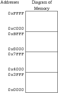
The memory map will consist of a diagram of the memory represented by stacked rectangles. Within the rectangles will be written the purpose or type of the memory at this location. The column to the left of the diagram will show the ranges for the different blocks of memory. For example, the top block in the memory map above ranges from address C00016 to FFFF16. If we represent these numbers in binary, we see that the range goes from 11000000000000002 to 11111111111111112. Notice that the first two bits remained the same. The last 14 bits covered the range from 0 to 3FFF16. This is a range of 2^14 = 16384 addresses (16K).
The Bus: The bus is an extension or slight modification of the internal structure of the processor including:
Since many devices are attached to the data lines of the bus, there needs to be a method to know which device is allowed to be connected at one time. In other words, if more than one device tries to write to the bus at the same time, this causes a problem called bus contention. For example, when memory device 1 is being read, memory device 2 should be "disconnected".
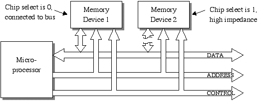
This disconnection is performed with tristate outputs. A tristate output is where one state is a logic 1, one state is a logic 0, and the third state is high impedance or open circuit. The third state is controlled by the chip select.
This disconnection is taken care of with a tri-state buffer that is placed at the end of each of the data lines. These buffers act as shown in the figure below. (Note that Z indicates an "open" or high impedance state.)
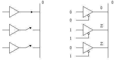
The end result should be that while multiple devices have their outputs connected to a common bus (i.e., many devices may be allowed to output data onto a single wire), only one is talking at any one time. The others are all disconnected from the wire so that their outputs don't corrupt the output of the device that has been given permission to talk by its low chip select.
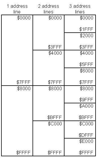
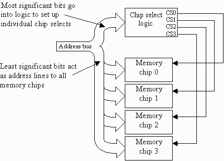
Rarely is only one type of memory or device connected to a bus, therefore, we need to develop circuitry to control the chip selects of each individual memory chip so that only one is "talking" on the data bus at a time. Address decoding is a method for dividing memory space into halves/fourths/eighths/etc. It uses logic to create a chip select signal for each piece of memory. The figure below shows how a memory map with addresses from hex 0000 to hex FFFF can be subdivided into pieces using the first 1, 2, or 3 address lines of the address bus.
The first step of address decoding is to separate a certain number of address lines from the most significant portion of the address, and dedicating them to the address decoding circuitry.
How do we design the chip select logic? I'm glad you asked. First, we need to figure out how many of those most significant bits it will take to address a certain range of memory. Let's do it with an example.
Assume that we have a total memory space from hex 0000 to hex FFFF and we want to create a chip select that resides in a portion of the memory space from hex C000 to hex DFFF. To create the chip select for this memory range, we want to look for the address lines that have one value inside the PROM�s address range and a different value outside the memory's address range. To do that, we want to look at the binary values of the address range (note the X�s represent "don�t care" values). The shaded areas of the table are the addresses of the memory's location.
|
Hex Address
|
Binary Address
|
Hex Address
|
Binary Address
|
|
0XXX
|
0000 XXXX XXXX XXXX
|
8XXX
|
1000 XXXX XXXX XXXX
|
|
1XXX
|
0001 XXXX XXXX XXXX
|
9XXX
|
1001 XXXX XXXX XXXX
|
|
2XXX
|
0010 XXXX XXXX XXXX
|
AXXX
|
1010 XXXX XXXX XXXX
|
|
3XXX
|
0011 XXXX XXXX XXXX
|
BXXX
|
1011 XXXX XXXX XXXX
|
|
4XXX
|
0100 XXXX XXXX XXXX
|
CXXX
|
1100 XXXX XXXX XXXX
|
|
5XXX
|
0101 XXXX XXXX XXXX
|
DXXX
|
1101 XXXX XXXX XXXX
|
|
6XXX
|
0110 XXXX XXXX XXXX
|
EXXX
|
1110 XXXX XXXX XXXX
|
|
7XXX
|
0111 XXXX XXXX XXXX
|
FXXX
|
1111 XXXX XXXX XXXX
|
Note that the low address of the range is 1100 0000 0000 0000 and the high end is 1101 1111 1111 1111. Examination of these two addresses reveal that the most significant three bits remain the same throughout the range. The lower 13 bits are the address lines that are to go to the memory chip. Therefore, our memory chip can have an address range of 2^13 = 8192 (8K).
We can also work this the other way around. Let's say we have 20 address lines. This gives us a 1 MEG (1,048,576) memory space. If we wanted to add a 16K (16384) memory to this memory space, how would we assign address lines?
First, 16,384 takes how many addresses? We figure this out by figuring out what power of two equals 16384. Since 2^14=16384, then we know that it takes 14 address lines to address 16K of memory.
Second, how many address lines does that leave for our chip select? Well, 20-14 leaves 6 address lines.
Third, how many 16K memories can we place inside a 1 MEG memory space. The easy way to do that is to divide 16,384 into 1,048,576 which gives us 64. Therefore, we could "stack" 64 16K memory chips into a 1 MEG memory space. We could also have figured this out by noting that there are 6 address lines available for chip selects. 2^6 = 64 wheich means we could make 64 different chip selects.
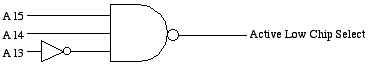
Now back to our example where we are trying to come up with the chip select for the range 0xC000 to 0xDFFF. There are 3 address lines we need to use for our chip select, A15, A14, and A13. A15 equals a 1, A14 equals a 1, and A13 equals a 0 in the range. Therefore, the equation should be A15 and A14 and not A13.
CS = A15 · A14 · ^ A13
There is one more thing we need to address. Chip selects are active low. In other words, they are zero when the address range is correct for the chip they are assigned to and 1 otherwise. Therefore, the equation above needs to be inverted.
CS = ^(A15 · A14 · ^ A13)
The logic diagram for this equation is:
In class, we will discuss how chip manufacturers designed the 74HC138 to make it easier on us to design chip selects. (That doesn't mean you won't need to know how to design chip selects for the test!)
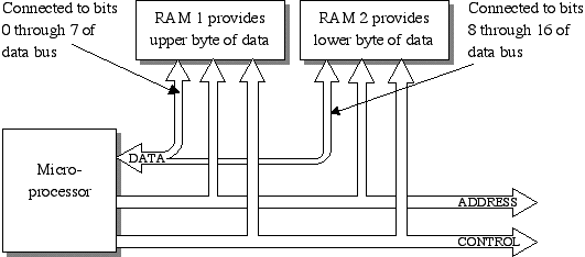
If your application needs 16 bits for data, but you only have 8 bit memories, you can expand the memories data bus by putting two memory chips in parallel. If you keep the address and control lines the same for both chips, then one will access the upper byte of data while the other accesses the lower byte of data. See the figure below.
Notes developed by David Tarnoff solely for use by students in his sections of CSCI 2150.